TC7WG02FC Overview
Key Features
- High output current : ±8 mA (min) at VCC = 3 V
- Super high speed operation: tpd = 2.8 ns (typ.) at VCC = 3.3 V, 15pF
- Operating voltage range : VCC = 0.9 to 3.6 V
- 5.5-V tolerant inputs
| Part | TC7WG02FC |
|---|---|
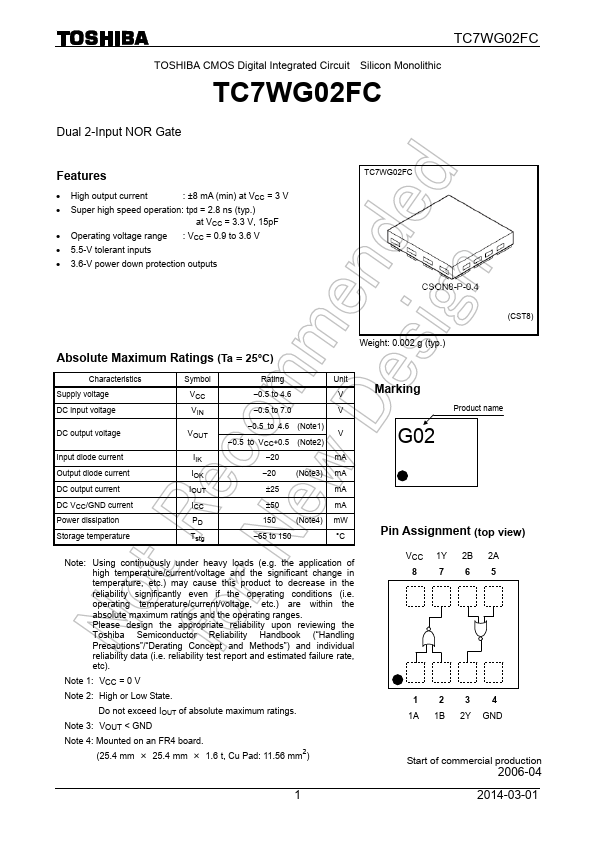
| Description | Dual 2-Input NOR Gate |
| Manufacturer | Toshiba |
| Size | 212.90 KB |
| Part Number | Manufacturer | Description |
|---|---|---|
| NSi6602 | NOVOSENSE | High Reliability Isolated Dual-Channel Gate Driver |
| NSi6801 | NOVOSENSE | Single-Channel Isolated Gate Driver |
| FD2103 | Fortior | 180V Half-Bridge Gate Driver |