Datasheet4U.com
🌙
TC7WPB8307L8X Datasheet | Toshiba
Part:
TC7WPB8307L8X
Description:
2-Bit Dual-Supply Bus Switch
Manufacturer:
Toshiba
Size:
240.89 KB
TC7WPB8307L8X Datasheet (PDF) Download
Toshiba
TC7WPB8307L8X
Key Features
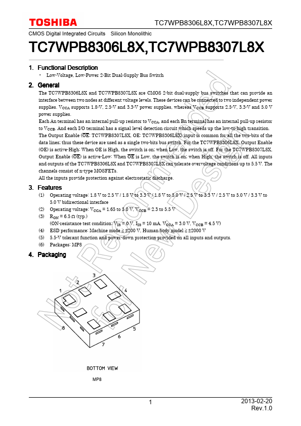
Packaging MP8 1 2013-02-20 Rev.1.0
Pin Assignment TC7WPB8306L8X TC7WPB8306L8X,TC7WPB8307L8X TC7WPB8307L8X
Marking TC7WPB8306L8X TC7WPB8307L8X
×
Close