TLP261J
TOSHIBA Photocoupler IRED + Photo-Triac
Triac Drivers Programmable Controllers AC-Output Modules Solid-State Relays
The TOSHIBA mini-flat coupler TLP261J is housed in a small-outline package and suitable for surface-mount assembly.
The TLP261J consists of an infrared emitting diode optically coupled to a triac-output photocoupler.
- Peak off-state voltage: 600 V (min)
- Trigger LED current: 10 m A (max)
- On-state current: 70 m A (max)
- Isolation voltage: 3000 Vrms (min)
- Zero-crossing function
- UL-recognized: UL 1577, File No.E67349
- VDE-approved: EN 60747-5-5 (Note 1)
Note 1: When a VDE approved type is needed, please designate the Option(V4).
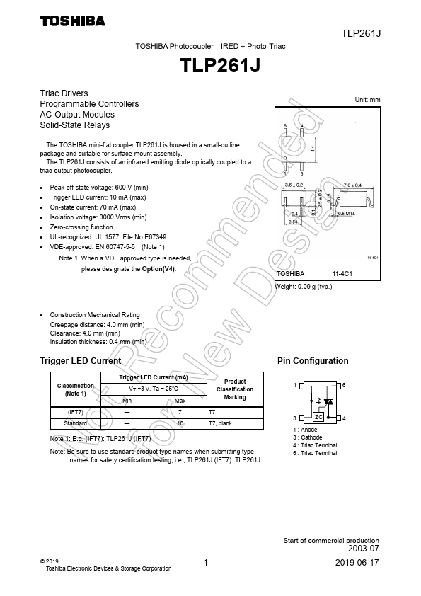
Unit: mm
TOSHIBA
11-4C1
Weight: 0.09 g (typ.)
- Construction Mechanical Rating
Creepage distance: 4.0 mm (min) Clearance: 4.0 mm (min) Insulation thickness: 0.4 mm (min)
Trigger LED Current
Classification (Note 1)
(IFT7) Standard
Trigger LED Current (m A)
VT =3 V, Ta = 25°C
Min
Max
―
―
Product...