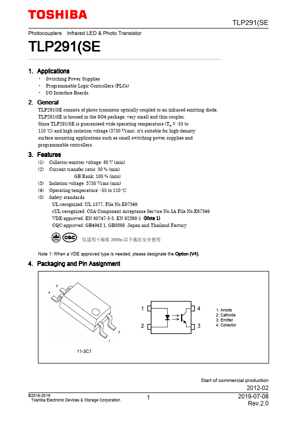
5. Mechanical Parameters
TLP291(SE
Characteristics
Creepage distances
Clearance
Internal isolation thickness
Min
Unit
5.0
mm
5.0
0.4
6. Absolute Maximum Ratings (Note) (Unless otherwise specified, Ta = 25 )
Characteristics
Symbol
Note
Rating
Unit
LED Input forward current
IF
50
mA
Input forward current derating
(Ta ≥ 90 )
∆IF/∆Ta
-1.5
mA/
Input forward current (pulsed)
IFP
(Note 1)
1
A
Input reverse voltage
VR
5
V
Input power dissipation
PD
100
mW
Input power dissipation derating
(Ta ≥ 90 )
∆PD/∆Ta
-3.0
mW/
Junction temperature
Tj
125
Detector Collector-emitter voltage
VCEO
80
V
Emitter-collector voltage
VECO
7
V
Collector current
IC
50
mA
Collector power dissipation
PC
150
mW
Collector power dissipation
derating
(Ta ≥ 25 )
∆PC/∆Ta
-1.5
mW/
Junction temperature
Tj
125
Common Operating temperature
Topr
-55 to 110
Storage temperature
Tstg
-55 to 125
Lead soldering temperature
(10 s)
Tsol
260
Total power dissipation
PT
200
mW
Total power dissipation derating
(Ta ≥ 25 )
∆PT/∆Ta
-2.0
mW/
Isolation voltage
AC, 60 s, R.H. ≤ 60 %
BVS
(Note 2)
3750
Vrms
Note: Using continuously under heavy loads (e.g. the application of high temperature/current/voltage and the
significant change in temperature, etc.) may cause this product to decrease in the reliability significantly even
if the operating conditions (i.e. operating temperature/current/voltage, etc.) are within the absolute maximum
ratings.
Please design the appropriate reliability upon reviewing the Toshiba Semiconductor Reliability Handbook
("Handling Precautions"/"Derating Concept and Methods") and individual reliability data (i.e. reliability test
report and estimated failure rate, etc).
Note 1: Pulse width (PW) ≤ 0.1 ms, f = 100 Hz
Note 2: This device is considered as a two-terminal device: Pins 1 and 2 are shorted together, and pins 3 and 4 are
shorted together.
7. Electrical Characteristics (Unless otherwise specified, Ta = 25 )
Characteristics
LED Input forward voltage
Input reverse current
Input capacitance
Detector Collector-emitter breakdown
voltage
Emitter-collector breakdown
voltage
Dark Current
Collector-emitter capacitance
Symbol
VF
IR
Ct
V(BR)CEO
Note
Test Condition
IF = 10 mA
VR = 5 V
V = 0 V, f = 1 MHz
IC = 0.5 mA
V(BR)ECO
IE = 0.1 mA
IDARK
CCE
VCE = 48 V
VCE = 48 V, Ta = 85
V = 0 V, f = 1 MHz
Min Typ. Max Unit
1.1 1.25 1.4
V
5
µA
30
pF
80
V
7
V
0.001 0.08 µA
2
50
10
pF
©2016-2019
Toshiba Electronic Devices & Storage Corporation
2
2019-07-08
Rev.2.0