TPD7102F
TPD7102F is 1-channel High-Side N channel Power MOSFET Gate Driver manufactured by Toshiba.
Features z Charge pump circuit is built in z The diagnosis function of the voltage between OUT1 and SOURCE is built in z Housed in the PS-8 package and supplied in embossed carrier tape.
SON8-P-0303-0.65 Weight: 0.017g (typ.)
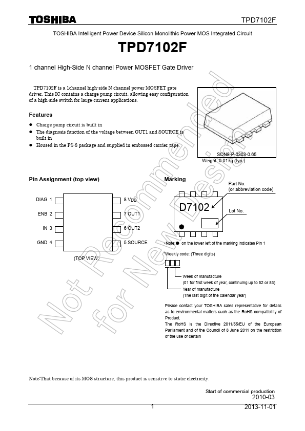
Pin Assignment (top view)
DIAG 1 ENB 2
IN 3 GND 4
(TOP VIEW)
8 VDD 7 OUT1 6 OUT2 5 SOURCE
Marking
D7102
Part No. (or abbreviation code)
Lot No.
- Note:- on the lower left of the marking indicates Pin 1
- Weekly code: (Three digits)
Week of manufacture (01 for first week of year, continuing up to 52 or 53) Year of manufacture (The last digit of the calendar year)
Please contact your TOSHIBA sales representative for details as to environmental matters such as the Ro HS patibility of Product. The Ro HS is the Directive 2011/65/EU of the European Parliament and of the Council of 8 June 2011 on the restriction of the use of certain
Note:That because of its MOS structure, this product is sensitive to static electricity.
Start of mercial production
2010-03
2013-11-01
Block Diagram / Application circuit
Regulator (VREG)
Output voltage protection
Constant 1m A → Current Driver
Charge pump
VDD+10V
Oscillation Circuit
ENB 5V
Input Logic OUT1-SOURCE voltage (VGS) monitor circuit
DIAG
Diagnosis Logic
Filter (2.2μs)
AMP 1/7
BATT
OUT1 OUT2
5kΩ 1MΩ
SOURCE...