Datasheet Summary
Bipolar Transistors Silicon NPN Triple-Diffused Type
1. Applications
- High-Speed High-Voltage Switching
- Switching Voltage Regulators
- High-Speed DC-DC Converters
2. Features
(1) High DC current gain: hFE = 100 to 200 (IC = 0.1 A) (2) High-speed switching: tf = 0.13 µs (typ.) (IC = 0.3 A)
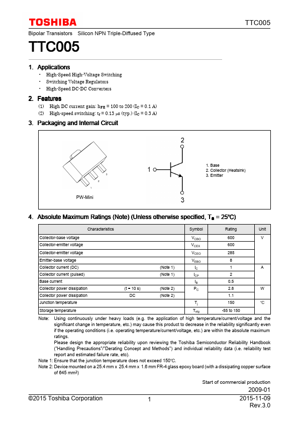
3. Packaging and Internal Circuit
1. Base 2. Collector (Heatsink) 3. Emitter
PW-Mini
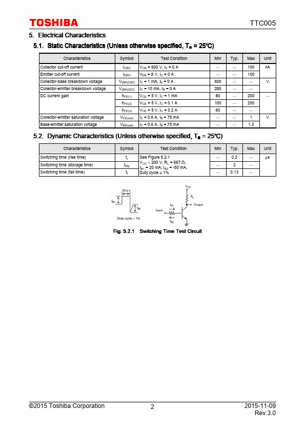
4....