2SK3316
Overview
2SK3316 TOSHIBA Field Effect Transistor Silicon N Channel MOS Type (π−MOSV) 2SK3316 Switching Regulator Applications Fast reverse recovery time Low drain−source ON resistance High forward transfer ad...
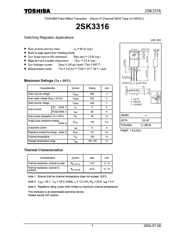
2SK3316 TOSHIBA Field Effect Transistor Silicon N Channel MOS Type (π−MOSV) 2SK3316 Switching Regulator Applications Fast reverse recovery time Low drain−source ON resistance High forward transfer ad...
| Part Number | Manufacturer | Description |
|---|---|---|
| 2SK3318 | Panasonic | Silicon N-channel power MOSFET |
| 2SK3310 | Inchange Semiconductor | N-Channel MOSFET Transistor |
| 2SK3313 | Inchange Semiconductor | N-Channel MOSFET Transistor |