HN1K06FU Overview
Key Specifications
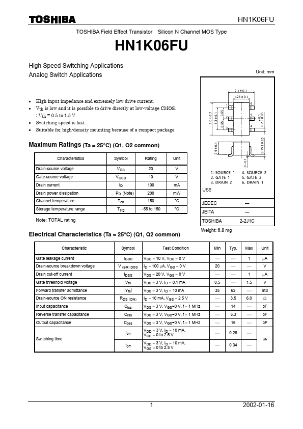
Pins: 6
Max Operating Temp: 150 °C
Key Features
- High input impedance and extremely low drive current. Vth is low and it is possible to drive directly at low-voltage CMOS. : Vth = 0.5 to 1.5 V Switching speed is fast. Suitable for high-density mounting because of a compact package