Datasheet Summary
TB2904HQ(o)
TOSHIBA Bi-CMOS Digital Integrated Circuit Silicon Monolithic
TB2904HQ (o)
Maximum Power 43 W BTL × 4-ch Audio Power IC
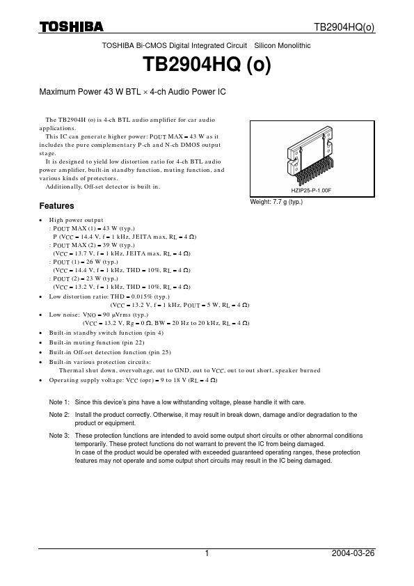
The TB2904H (o) is 4-ch BTL audio amplifier for car audio applications. This IC can generate higher power: POUT MAX = 43 W as it includes the pure plementary P-ch and N-ch DMOS output stage. It is designed to yield low distortion ratio for 4-ch BTL audio power amplifier, built-in standby function, muting function, and various kinds of protectors. Additionally, Off-set detector is built in.
Features
- High power output : POUT MAX (1) = 43 W (typ.) P (VCC = 14.4 V, f = 1 kHz, JEITA max, RL = 4 Ω) : POUT MAX (2) = 39 W (typ.) (VCC = 13.7 V, f = 1 kHz, JEITA...


