TC551001BTRL-70L Overview
Description
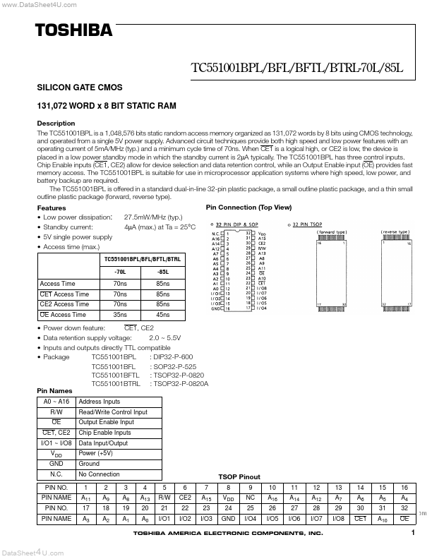
The TC551001BPL is a 1,048,576 bits static random access memory organized as 131,072 words by 8 bits using CMOS technology, and operated from a single 5V power supply. Advanced circuit techniques provide both high speed and low power features with an operating current of 5mA/MHz (typ.) and a minimum cycle time of 70ns.
Key Features
- Low power dissipation: 27.5mW/MHz (typ.)
- Standby current: 4µA (max.) at Ta = 25°C
- 5V single power supply
- Access time (max.) TC551001BPL/BFL/BFTL/BTRL
- Power down feature: CE1, CE2
- Data retention supply voltage: 2.0 ~ 5.5V
- Inputs and outputs directly TTL compatible