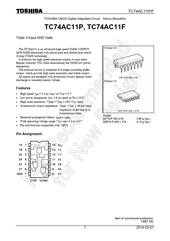
Datasheet4U Logo Datasheet4U.com

TC74AC11FN - Triple 3-Input AND Gate

This page provides the datasheet information for the TC74AC11FN, a member of the TC74AC11F Triple 3-Input AND Gate family.

Features

  • High speed: tpd = 5.3 ns (typ. ) at VCC = 5 V.
  • Low power dissipation: ICC = 4 μA (max) at Ta = 25°C.
  • High noise immunity: VNIH = VNIL = 28% VCC (min).
  • Symmetrical output impedance: |IOH| = IOL = 24 mA (min) Capability of driving 50 Ω transmission lines.
  • Balanced propagation delays: tpLH ∼.
  • tpHL.
  • Wide operating voltage range: VCC (opr) = 2 to 5.5 V.
  • Pin and function compatible with 74F11 Pin Assignment Note: xxxFN (JEDEC SOP.

📥 Download Datasheet

Datasheet preview – TC74AC11FN

Datasheet Details

Part number TC74AC11FN
Manufacturer Toshiba
File Size 260.63 KB
Description Triple 3-Input AND Gate
Datasheet download datasheet TC74AC11FN Datasheet
Additional preview pages of the TC74AC11FN datasheet.
Other Datasheets by Toshiba Semiconductor

Full PDF Text Transcription

Click to expand full text
TC74AC11P/F/FN TOSHIBA CMOS Digital Integrated Circuit Silicon Monolithic TC74AC11P,TC74AC11F,TC74AC11FN Triple 3-Input AND Gate The TC74AC11 is an advanced high speed CMOS 3-INPUT AND GATE fabricated with silicon gate and double-layer metal wiring C2MOS technology. It achieves the high speed operation similar to equivalent Bipolar Schottky TTL while maintaining the CMOS low power dissipation. The internal circuit is composed of 4 stages including buffer output, which provide high noise immunity and stable output. All inputs are equipped with protection circuits against static discharge or transient excess voltage. Features • High speed: tpd = 5.3 ns (typ.
Published: |