Datasheet4U Logo Datasheet4U.com

TC74LVX174FT - Hex D-Type Flip-Flop

Download the TC74LVX174FT datasheet PDF. This datasheet also covers the TC74LVX174F variant, as both devices belong to the same hex d-type flip-flop family and are provided as variant models within a single manufacturer datasheet.

Features

  • High-speed: fmax = 180 MHz (typ. ) (VCC = 3 V).
  • Low power dissipation: ICC = 4 μA (max) (Ta = 25°C).
  • Input voltage level: VIL = 0.8 V (max) (VCC = 3 V) VIH = 2.0 V (min) (VCC = 3 V).
  • Power-down protection provided on all inputs.
  • Balanced propagation delays: tpLH ∼.
  • tpHL.
  • Low noise: VOLP = 0.5 V (max).
  • Pin and function compatible with 74HC174 TC74LVX174F TC74LVX174FT Weight SOP16-P-300-1.27A TSSOP16-P-0044-0.65A : 0.18 g (.

📥 Download Datasheet

Note: The manufacturer provides a single datasheet file (TC74LVX174F_ToshibaSemiconductor.pdf) that lists specifications for multiple related part numbers.

Full PDF Text Transcription (Reference)

The following content is an automatically extracted verbatim text from the original manufacturer datasheet and is provided for reference purposes only.

View original datasheet text
TC74LVX174F/FT TOSHIBA CMOS Digital Integrated Circuit Silicon Monolithic TC74LVX174F, TC74LVX174FT 
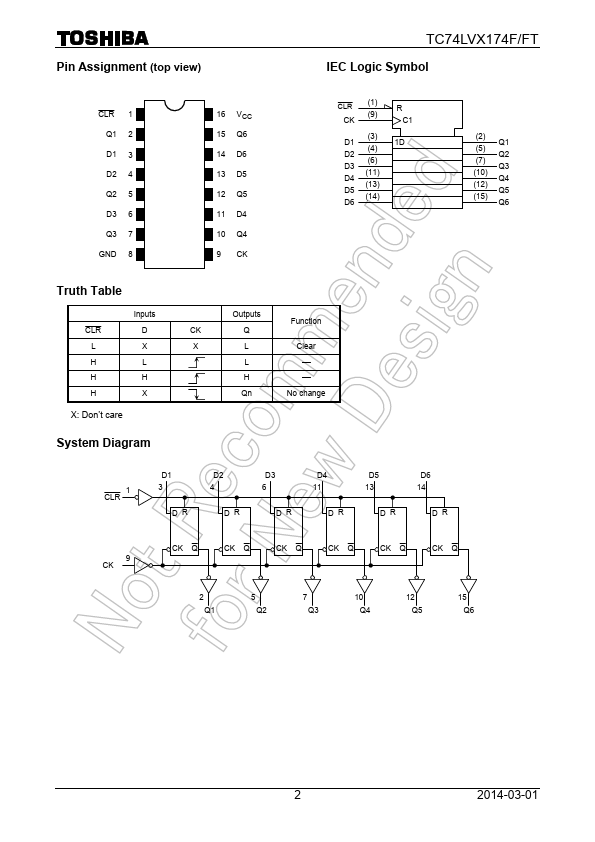
Hex D-Type Flip-Flop with Clear The TC74LVX174F/FT is a high-speed CMOS hex D-flip flop fabricated with silicon gate CMOS technology. Designed for use in 3-V systems, it achieves high-speed operation while maintaining the CMOS low power dissipation. This device is suitable for low voltage and battery operated systems. Information signals applied to D inputs are transfered to the Q output on the positivegoing edge of the clock pulse. When the CLR input is held low, the Q output are in the low logic level independent of the other inputs. An input protection circuit ensures that 0 to 5.5V can be applied to the input pins without regard to the supply voltage.
Published: |