TC7SP302WBG
TC7SP302WBG is Dual supply 2-Input NOR Gate manufactured by Toshiba.
TOSHIBA CMOS Digital Integrated Circuit Silicon Monolithic
Dual supply 2-Input NOR Gate with Level Translator
The TC7SP302 is a dual supply, advanced high-speed CMOS 2-input dual supply voltage interface NOR gate fabricated with silicon gate CMOS technology.
It is also designed with over voltage tolerant inputs and outputs up to 3.6 V.
Designed for use as an interface between a 1.2-V, 1.5-V, 1.8-V, or 2.5-V bus and a 1.8-V, 2.5-V or 3.3-V bus in mixed 1.2-V, 1.5-V, 1.8-V or 2.5-V/1.8-V, 2.5-V or 3.3-V supply systems.
All inputs are equipped with protection circuits against static discharge.
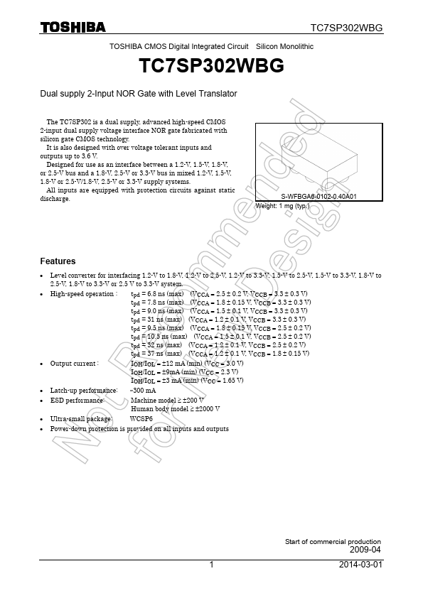
S-WFBGA6-0102-0.40A01 Weight: 1 mg (typ.)
Features
- Level converter for interfacing 1.2-V to 1.8-V, 1.2-V to 2.5-V, 1.2-V to 3.3-V, 1.5-V to 2.5-V, 1.5-V to 3.3-V, 1.8-V to 2.5-V, 1.8-V to 3.3-V or 2.5 V to 3.3-V system.
- High-speed operation : tpd = 6.8 ns (max) (VCCA = 2.5 ± 0.2 V, VCCB = 3.3 ± 0.3 V) tpd = 7.8 ns (max) (VCCA = 1.8 ± 0.15 V, VCCB = 3.3 ± 0.3 V) tpd = 9.0 ns (max) (VCCA = 1.5 ± 0.1 V, VCCB = 3.3 ± 0.3 V) tpd = 31 ns (max) (VCCA = 1.2 ± 0.1 V, VCCB = 3.3 ± 0.3 V) tpd = 9.5 ns (max) (VCCA = 1.8 ± 0.15 V, VCCB = 2.5 ± 0.2 V) tpd = 10.5 ns (max) (VCCA = 1.5 ± 0.1 V, VCCB = 2.5 ± 0.2 V) tpd = 32 ns (max) (VCCA = 1.2 ± 0.1 V, VCCB = 2.5 ± 0.2 V) tpd = 37 ns (max) (VCCA = 1.2 ± 0.1 V, VCCB = 1.8 ± 0.15 V)
- Output current :
IOH/IOL = ±12 m A (min) (VCC = 3.0 V) IOH/IOL = ±9m A (min) (VCC = 2.3 V) IOH/IOL = ±3 m A (min) (VCC = 1.65 V)
- Latch-up performance: -300 m A
- ESD performance:
Machine model ≥ ±200 V Human body model ≥ ±2000 V
- Ultra-small package:
WCSP6
- Power-down protection is provided on all inputs and outputs
Start of mercial production
2009-04
2014-03-01
Pin Assignment (top view)
VCCA GND A
- B
VCCB B
Truth Table
Inputs
Block Diagram
- Output
Y H L L...