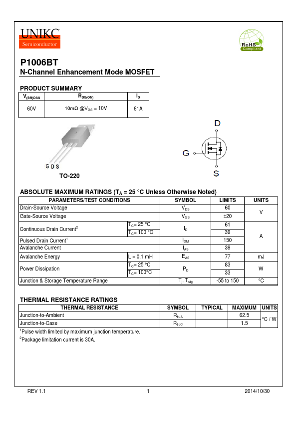
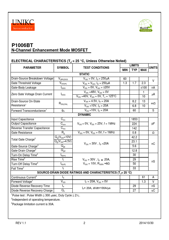
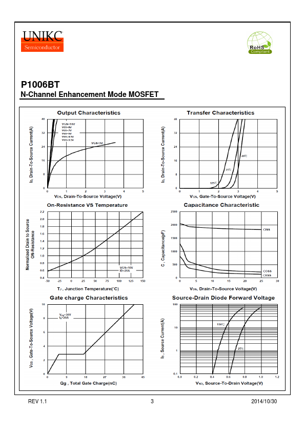
Click to expand full text
P1006BT
N-Channel Enhancement Mode MOSFET
PRODUCT SUMMARY
V(BR)DSS
RDS(ON)
ID
60V
10mΩ @VGS = 10V
61A
TO-220
ABSOLUTE MAXIMUM RATINGS (TA = 25 °C Unless Otherwise Noted)
PARAMETERS/TEST CONDITIONS
SYMBOL
LIMITS
Drain-Source Voltage
VDS
60
Gate-Source Voltage
VGS
±20
Continuous Drain Current2 Pulsed Drain Current1
TC= 25 °C TC= 100 °C
ID
61 39
IDM
150
Avalanche Current
IAS
39
Avalanche Energy
L = 0.1 mH
EAS
77
Power Dissipation
TC= 25 °C TC= 100°C
PD
83 33
Junction & Storage Temperature Range
Tj, Tstg
-55 to 150
UNITS V
A
mJ W °C
THERMAL RESISTANCE RATINGS
THERMAL RESISTANCE Junction-to-Ambient Junction-to-Case 1Pulse width limited by maximum junction temperature. 2Package limitation current is 30A.
SYMBOL RqJA RqJC
TYPICAL
MAXIMUM 62.5 1.