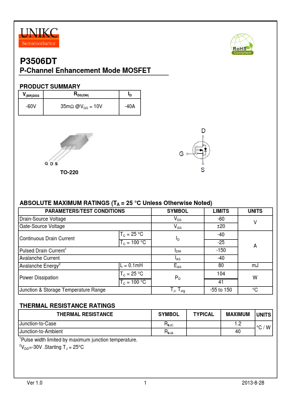
P3506DT Description
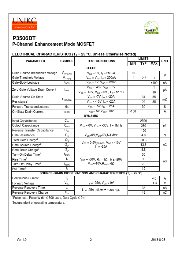
Pulse Width 300 msec, Duty Cycle 2%. 2Independent of operating temperature.
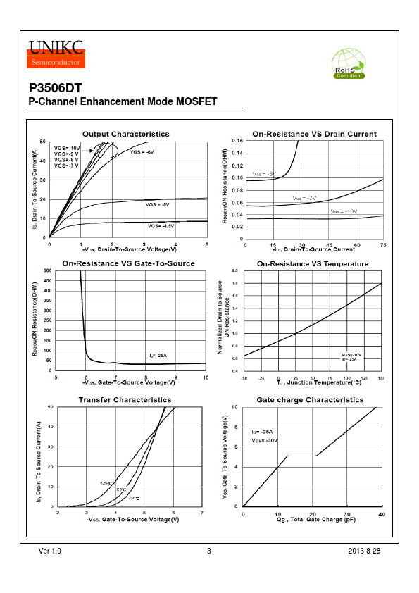
P3506DT is P-Channel MOSFET manufactured by UNIKC.
| Manufacturer | Part Number | Description |
|---|---|---|
| P3506DT | P-Channel Transistor | |
| P3506DTF | P-Channel Transistor | |
| P3506DD | P-Channel Transistor | |
| P3506ETF | P-Channel Field Effect Transistor |
Pulse Width 300 msec, Duty Cycle 2%. 2Independent of operating temperature.