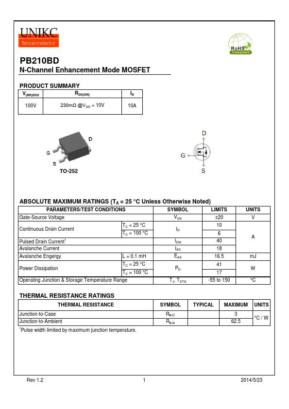
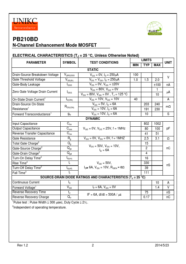
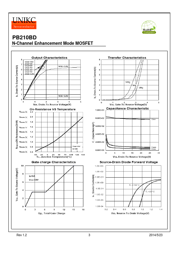
Click to expand full text
PB210BD
N-Channel Enhancement Mode MOSFET
PRODUCT SUMMARY
V(BR)DSS
RDS(ON)
ID
100V
230mΩ @VGS = 10V
10A
TO-252
ABSOLUTE MAXIMUM RATINGS (TA = 25 °C Unless Otherwise Noted)
PARAMETERS/TEST CONDITIONS
SYMBOL
LIMITS
Gate-Source Voltage
VGS
±20
Continuous Drain Current Pulsed Drain Current1
TC = 25 °C
ID
10
TC = 100 °C
6
IDM
40
Avalanche Current
IAS
18
Avalanche Engergy
L = 0.1 mH
EAS
16.5
Power Dissipation
TC = 25 °C
PD
41
TC = 100 °C
17
Operating Junction & Storage Temperature Range
TJ, TSTG
-55 to 150
UNITS V
A
mJ W °C
THERMAL RESISTANCE RATINGS
THERMAL RESISTANCE
Junction-to-Case Junction-to-Ambient 1Pulse width limited by maximum junction temperature.
SYMBOL
RqJC RqJA
TYPICAL
MAXIMUM 3
62.5
UNITS °C / W
Rev 1.