Datasheet Summary
ą
D Integrated 0.15-Ω Power MOSFET D 3-V to 8-V Operation D Digital Programmable Current Limit from 0 A to 3 A
D Electronic Circuit Breaker Function D 1µA ICC When Disabled D Programmable On-Time D Programmable Start Delay D Fixed 3% Duty Cycle
UCC2912 UCC3912 PROGRAMMABLE HOT SWAP POWER MANAGER
SLUS241D
- MARCH 1994
- REVISED NOVEMBER 2003
D Unidirectional Switch D Thermal Shutdown D Fault-Output Indicator D Maximum-Output Current Can Be Set to 1 A
Above the Programmed Fault Level or to a Full 4 A
D Power SOIC, Low-Thermal Resistance
Packaging description
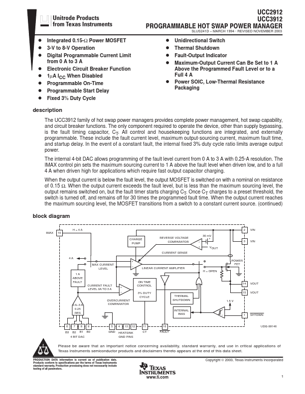
The UCC3912 family of hot swap power managers provides plete power management, hot swap capability, and circuit breaker functions....