MBR20100CT-N3
Description
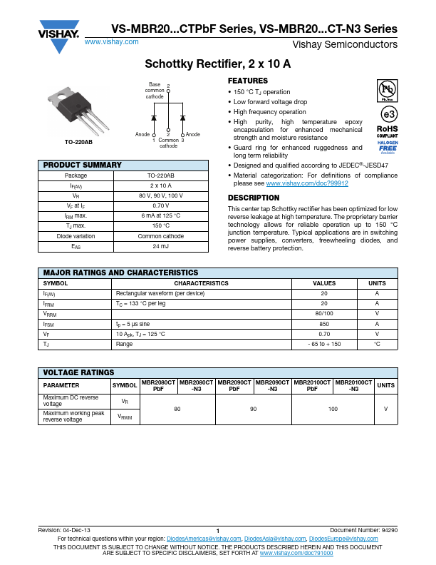
This center tap Schottky rectifier has been optimized for low reverse leakage at high temperature. The proprietary barrier technology allows for reliable operation up to 150 °C junction temper.
Key Features
- 150 °C TJ operation
- Low forward voltage drop
- High frequency operation
- High purity, high temperature epoxy encapsulation for enhanced mechanical strength and moisture resistance
- Guard ring for enhanced ruggedness and long term reliability Available
- Designed and qualified according to JEDEC®-JESD47
- Material categorization: For definitions of pliance please see .vishay./doc?99912