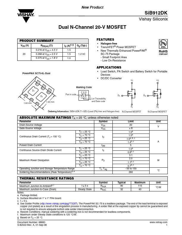
SIB912DK
SIB912DK is Dual N-Channel MOSFET manufactured by Vishay.
FEATURES
- Halogen-free
- Trench FET® Power MOSFET
- New Thermally Enhanced Power PAK® SC-75 Package
- Small Footprint Area
- Low On-Resistance
Ro HS
PLIANT
APPLICATIONS
Power PAK SC75-6L-Dual
- Load Switch, PA Switch and Battery Switch for Portable Devices
- DC/DC Converter
D1 D2
1 S1 2 G1 D1 D1 6 5 1.60 mm G2 4 S2 1.60 mm D2 D2 3 CAX Part # code XXX Lot Traceability and Date code G1
Marking Code
G2
S1 Ordering Information: Si B912DK-T1-GE3 (Lead (Pb)-free and Halogen-free) N-Channel MOSFET
S2 N-Channel MOSFET
ABSOLUTE MAXIMUM RATINGS TA = 25 °C, unless otherwise noted
Parameter Drain-Source Voltage Gate-Source Voltage TC = 25 °C TC = 70 °C TA = 25 °C TA = 70 °C TC = 25 °C TA = 25 °C TC = 25 °C TC = 70 °C TA = 25 °C TA = 70 °C http://..net/
Symbol VDS VGS ID
Limit 20 ±8 1.5a 1.5a 1.5a, b, c 1.4b, c 5 1.5a 0.9b, c 3.1 2.0 1.1b, c 0.7b, c
- 55 to 150 260
Unit V
Continuous Drain Current (TJ = 150 °C)
Pulsed Drain Current Continuous Source-Drain Diode Current
IDM IS
Maximum Power Dissipation
PD TJ, Tstg
Operating Junction and Storage Temperature Range Soldering Remendations (Peak Temperature)d, e
°C
THERMAL RESISTANCE RATINGS
Symbol Typical Maximum Unit t≤5s Rth JA 90 115 Maximum Junction-to-Ambientb, f °C/W Rth JC Maximum Junction-to-Case (Drain) Steady State 32 40 Notes: a. Package limited. b. Surface Mounted on 1" x 1" FR4 board. c. t = 5 s. d. See Solder Profile (http://.vishay./ppg?73257). The Power PAK SC-75 is a leadless package. The end of the lead terminal is exposed copper (not plated) as a result of the singulation process in manufacturing. A solder fillet at the exposed copper tip cannot be guaranteed and is not required to ensure adequate bottom side solder interconnection. e. Rework Conditions: manual soldering with a soldering iron is not remended for leadless ponents. f. Maximum under Steady State conditions is 125 °C/W. g. Based on TC = 25 °C. Document Number: 68883 S-82022-Rev. A, 01-Sep-08 .vishay. 1 datasheet pdf
-...