X25040 Overview
Key Specifications
Package: SOP
Operating Voltage: 5 V
Max Voltage (typical range): 5.5 V
Min Voltage (typical range): 4.5 V
Key Features
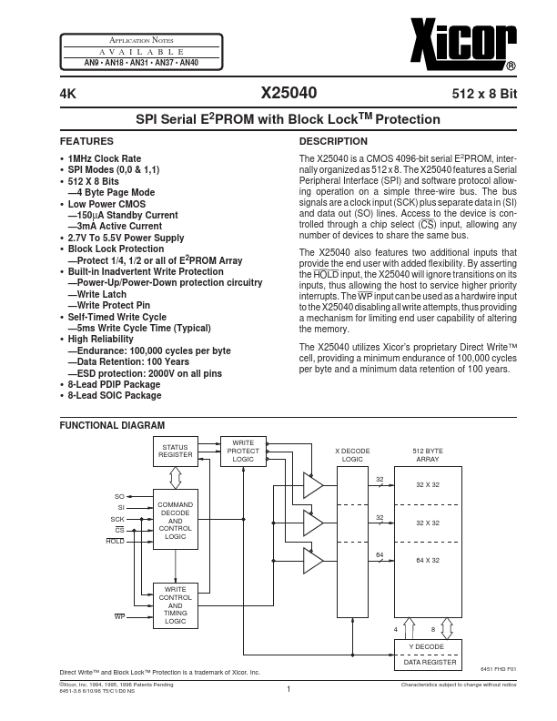
- The bus signals are a clock input (SCK) plus separate data in (SI) and data out (SO) lines
- Access to the device is controlled through a chip select (CS) input, allowing any number of devices to share the same bus
- The X25040 also features two additional inputs that provide the end user with added flexibility
- By asserting the HOLD input, the X25040 will ignore transitions on its inputs, thus allowing the host to service higher priority interrupts