Datasheet Summary
<BL Blue>
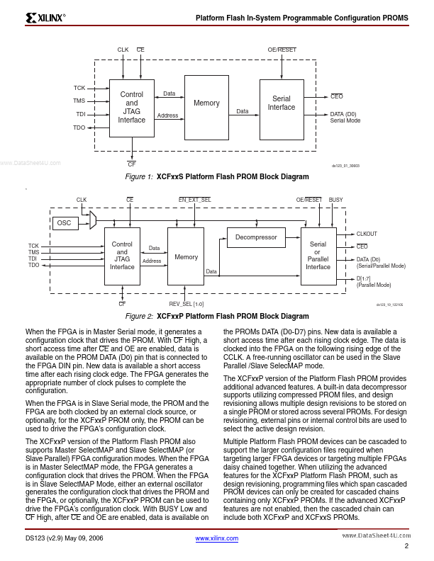
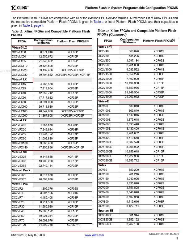
Platform Flash In-System Programmable Configuration PROMS
Product Specification
DS123 (v2.9) May 09, 2006
Features
- -
- - In-System Programmable PROMs for Configuration of Xilinx FPGAs Low-Power Advanced CMOS NOR FLASH Process Endurance of 20,000 Program/Erase Cycles Operation over Full Industrial Temperature Range (- 40°C to +85°C) Boundary-Scan (JTAG) Support for Programming, Prototyping, and Testing JTAG mand Initiation of Standard FPGA Configuration Cascadable for Storing Longer or Multiple Bitstreams Dedicated Boundary-Scan (JTAG) I/O Power Supply (VCCJ) I/O Pins patible with Voltage Levels Ranging From 1.5V to 3.3V Design Support Using the Xilinx Alliance ISE...