ADS5400
ADS5400 is 1-GSPS Analog-to-Digital Converter manufactured by Texas Instruments.
Features
- 1 1-GSPS Sample Rate
- 12-Bit Resolution
- 2.1 GHz Input Bandwidth
- SFDR = 66 d Bc at 1.2 GHz
- SNR = 57.6 d BFS at 1.2 GHz
- 7 Clock Cycle Latency
- Interleave Friendly: Internal Adjustments for Gain,
Phase, and Offset
- 1.5-V to 2-V Selectable Full-Scale Range
- LVDS-patible Outputs, 1 or 2 Bus Options
- Total Power Dissipation: 2.15 W
- On-Chip Analog Buffer
- 100-Pin HTQFP Power PAD™ Package
(16-mm × 16-mm Footprint With Leads)
- Industrial Temperature Range of
- 40°C to 85°C
2 Applications
- Test and Measurement Instrumentation
- Ultra-Wide Band Software-Defined Radio
- Data Acquisition
- Power Amplifier Linearization
- Signal Intelligence and Jamming
- Radar
3 Description
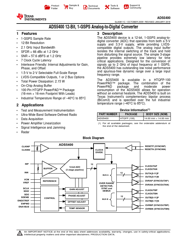
The ADS5400 device is a 12-bit, 1-GSPS analog-todigital converter (ADC) that operates from both a 5-V supply and 3.3-V supply, while providing LVDSpatible digital outputs. The analog input buffer isolates the internal switching of the track and hold from disturbing the signal source. The simple 3-stage pipeline provides extremely low latency for time critical applications. Designed for the conversion of signals up to 2 GHz of input frequency at 1 GSPS, the ADS5400 has outstanding low noise performance and spurious-free dynamic range over a large input frequency range.
The ADS5400 is available in a HTQFP-100 Power PAD™ package. The bination of the Power PAD package and moderate power consumption of the ADS5400 allows for operation without an external heatsink. The ADS5400 is built on Texas Instrument's plementary bipolar process (Bi3) and is specified over the full industrial temperature range (- 40°C to 85°C).
PART NUMBER ADS5400
Device Information(1)
PACKAGE
BODY SIZE (NOM)
HTQFP (100)
14.00 mm × 14.00 mm
(1) For all available packages, see the orderable addendum at the end of the datasheet.
Block Diagram
CLKINP CLKINN
CLOCK DIVIDE
RESETP (SYNCINP) RESETN...