CD54HCT257 Overview
Key Specifications
Package: CDIP
Mount Type: Through Hole
Pins: 16
Operating Voltage: 5 V
Description
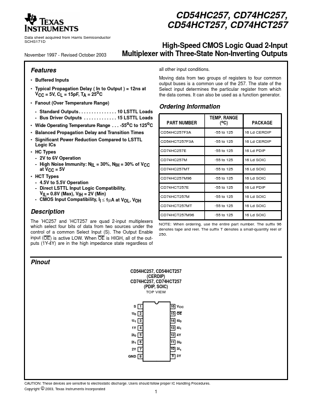
The ’HC257 and ’HCT257 are quad 2-input multiplexers which select four bits of data from two sources under the control of a common Select Input (S). The Output Enable input (OE) is active LOW.
Key Features
- Buffered Inputs
- Typical Propagation Delay ( In to Output ) = 12ns at VCC = 5V, CL = 15pF, TA = 25oC
- Fanout (Over Temperature Range)
- Standard Outputs . . . . . . . . . . . . . . . 10 LSTTL Loads
- Bus Driver Outputs . . . . . . . . . . . . . 15 LSTTL Loads