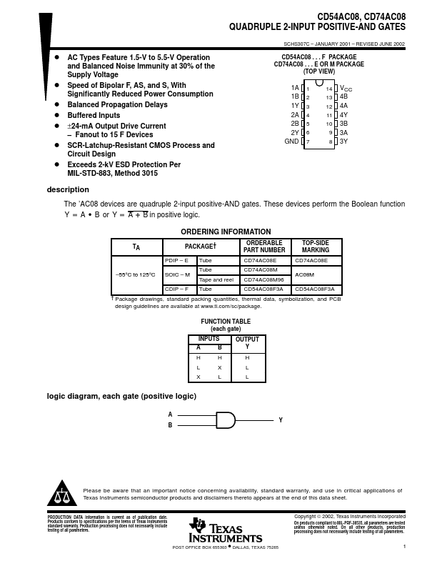
CD74AC08
Feature
1.5-V to 5.5-V Operation and Balanced Noise Immunity at 30% of the
Supply Voltage
D Speed of Bipolar F, AS, and S, With
Significantly Reduced Power Consumption
D Balanced Propagation Delays D Buffered Inputs D ±24-m A Output Drive Current
- Fanout to 15 F Devices
D SCR-Latchup-Resistant CMOS Process and
Circuit Design
D Exceeds 2-k V ESD Protection Per
MIL-STD-883, Method 3015
SCHS307C
- JANUARY 2001
- REVISED JUNE 2002
CD54AC08 . . . F PACKAGE CD74AC08 . . . E OR M PACKAGE
(TOP VIEW)
1A 1B 1Y 2A 2B 2Y GND
1 2 3 4 5 6 7
14 VCC 13 4B 12 4A 11 4Y 10 3B 9 3A 8 3Y description
The ’AC08 devices are quadruple 2-input positive-AND gates. These devices perform the Boolean function
+ + )Y A
- B or Y A B in positive logic.
ORDERING INFORMATION
PACKAGE†
ORDERABLE PART NUMBER
TOP-SIDE MARKING
PDIP
- E Tube
CD74AC08E
CD74AC08E
Tube
- 55°C to 125°C SOIC
- M
Tape and reel
CD74AC08M CD74AC08M96
AC08M
CDIP
- F Tube
CD54AC08F3A...