CD74HCT373
Features
- 4.5-V to 5.5-V VCC operation
- Wide operating temperature range of
- 55°C to 125°C
- Balanced propagation delays and transition times
- Standard outputs drive up to 10 LS-TTL loads
- Significant power reduction pared to LS-TTL
Logic ICs
- Inputs are TTL-voltage patible
2 Description
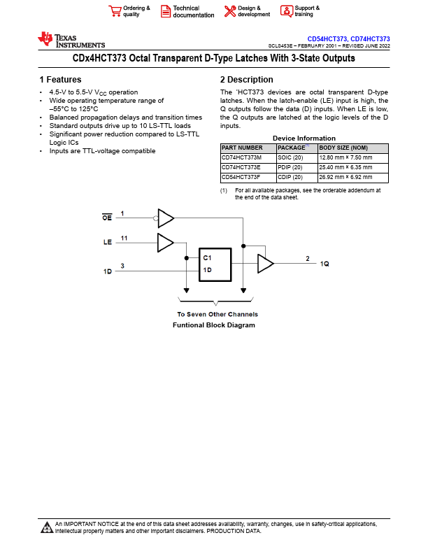
The ’HCT373 devices are octal transparent D-type latches. When the latch-enable (LE) input is high, the Q outputs follow the data (D) inputs. When LE is low, the Q outputs are latched at the logic levels of the D inputs.
PART NUMBER CD74HCT373M CD74HCT373E CD54HCT373F
Device Information
PACKAGE(1) BODY SIZE (NOM)
SOIC (20)
12.80 mm × 7.50 mm
PDIP (20)
25.40 mm × 6.35 mm
CDIP (20)
26.92 mm × 6.92 mm
(1) For all available packages, see the orderable addendum at the end of the data sheet.
Funtional Block Diagram
An IMPORTANT NOTICE at the end of this data sheet addresses availability, warranty, changes, use in safety-critical applications, intellectual property matters and other important disclaimers. PRODUCTION DATA.
CD54HCT373,...