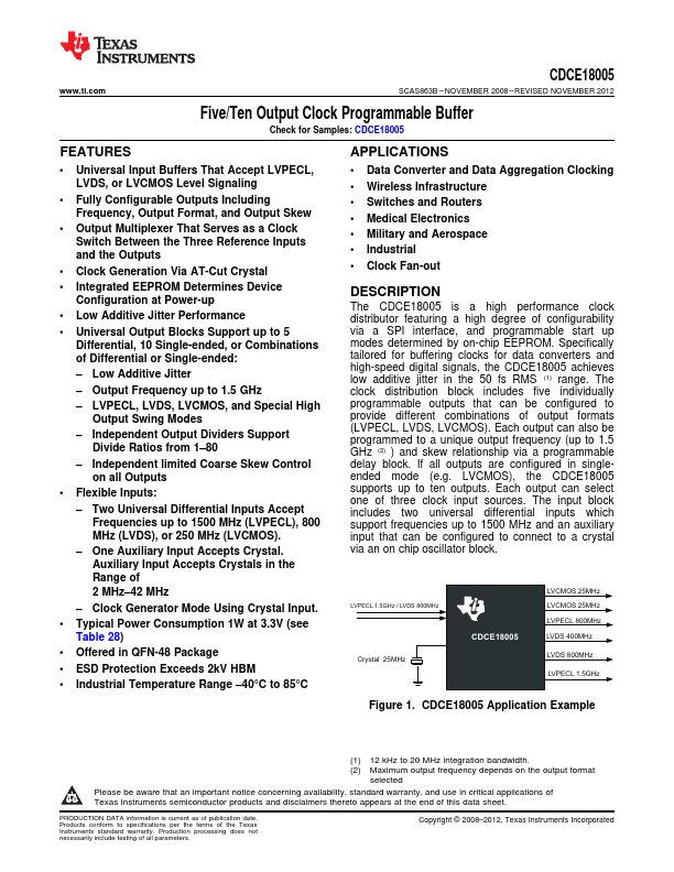
Datasheet Summary
.ti.
SCAS863B
- NOVEMBER 2008
- REVISED NOVEMBER 2012
Five/Ten Output Clock Programmable Buffer
Check for Samples: CDCE18005
Features
- Universal Input Buffers That Accept LVPECL, LVDS, or LVCMOS Level Signaling
- Fully Configurable Outputs Including Frequency, Output Format, and Output Skew
- Output Multiplexer That Serves as a Clock Switch Between the Three Reference Inputs and the Outputs
- Clock Generation Via AT-Cut Crystal
- Integrated EEPROM Determines Device
Configuration at Power-up
- Low Additive Jitter Performance
- Universal Output Blocks Support up to 5
Differential, 10 Single-ended, or binations of Differential or Single-ended:
- Low Additive Jitter
-...