CDCLVD1208
Overview
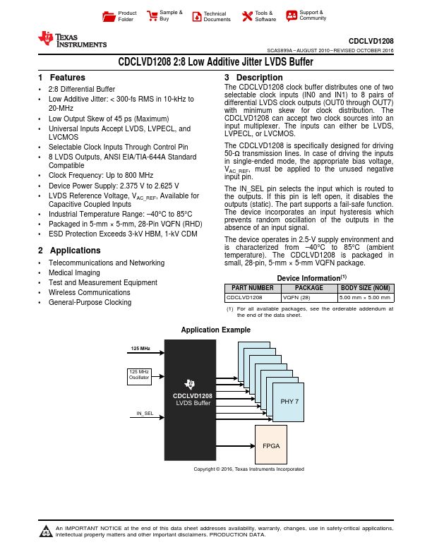
The CDCLVD1208 clock buffer distributes one of two selectable clock inputs (IN0 and IN1) to 8 pairs of differential LVDS clock outputs (OUT0 through OUT7) with minimum skew for clock distribution. The CDCLVD1208 can accept two clock sources into an input multiplexer.
- 1 2:8 Differential Buffer
- Low Additive Jitter: < 300-fs RMS in 10-kHz to 20-MHz
- Low Output Skew of 45 ps (Maximum)
- Universal Inputs Accept LVDS, LVPECL, and LVCMOS
- Selectable Clock Inputs Through Control Pin
- 8 LVDS Outputs, ANSI EIA/TIA-644A Standard Compatible
- Clock Frequency: Up to 800 MHz
- Device Power Supply: 2.375 V to 2.625 V
- LVDS Reference Voltage, VAC_REF, Available for Capacitive Coupled Inputs
- Industrial Temperature Range: -40°C to 85°C