CSD13202Q2
Overview
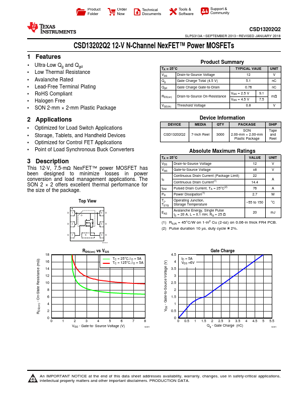
This 12-V, 7.5-mΩ NexFET™ power MOSFET has been designed to minimize losses in power conversion and load management applications. The SON 2 × 2 offers excellent thermal performance for the size of the package.
- 1 Ultra-Low Qg and Qgd
- Low Thermal Resistance
- Avalanche Rated
- Lead-Free Terminal Plating
- RoHS Compliant
- Halogen Free
- SON 2-mm × 2-mm Plastic Package Product Summary TA = 25°C VDS Drain-to-Source Voltage Qg Gate Charge Total (4.5 V) Qgd Gate Charge Gate-to-Drain RDS(on) Drain-to-Source On-Resistance VGS(th) Threshold Voltage