CSD16408Q5 Overview
Key Specifications
Mount Type: Surface Mount
Pins: 8
Height: 1.05 mm
Length: 5 mm
Description
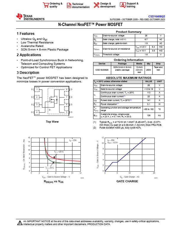
The NexFET™ power MOSFET has been designed to minimize losses in power conversion applications. S1 8D S2 7D S3 G4 D Top View 6D 5D P0094-01 16 14 12 10 8 6 4 2 0 0 ID = 25A TC = 125°C TC = 25°C 2 4 6 8 10 VGS - Gate to Source Voltage - V RDS(on) vs VGS 12 G006 Product Summary VDS Drain-to-source voltage 25 V Qg Gate charge, total (4.5 V) 6.7 nC Qgd Gate charge, gate-to-drain 1.9 nC rDS(on) Drain-to-source on-resistance VGS = 4.5 V VGS = 10 V 5.4 mΩ 3.6 mΩ VGS(th) Threshold voltage 1.8 V Device CSD16408Q5.
Key Features
- Ultralow Qg and Qgd
- Low - Avalanche Rated
- SON 5-mm × 6-mm Plastic Package