CSD17311Q5
Overview
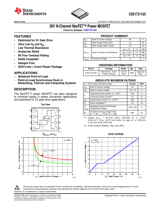
The NexFET™ power MOSFET has been designed to minimize losses in power conversion applications and optimized for 5V gate drive applications. Top View S1 8D S2 7D S3 G4 6 5 4 3 6D 5D P0094-01 RDS(on) vs VGS ID = 30A TC = 125°C 2 1 TC = 25°C 0 0 1 2 3 4 5 6 7 8 9 10 VGS - Gate-to-Source Voltage - V G006 VDS Qg Qgd RDS(on) VGS(th) PRODUCT SUMMARY Drain to Source Voltage 30 Gate Charge Total (4.5V) 24 Gate Charge Gate to Drain 5.2 Drain to Source On Resistance Threshold Voltage VGS = 3V VGS = 4.5V VGS = 8V 1.2 V nC nC 2.3 mΩ 1.8 mΩ 1.6 mΩ V.
- 2 Optimized for 5V Gate Drive
- Ultra Low Qg and Qgd
- Low Thermal Resistance
- Avalanche Rated
- Pb Free Terminal Plating
- RoHS Compliant
- Halogen Free
- SON 5-mm × 6-mm Plastic Package