CSD17585F5
CSD17585F5 is N-Channel MOSFET manufactured by Texas Instruments.
Features
- 1 Low-On Resistance
- Ultra-Low Qg and Qgd
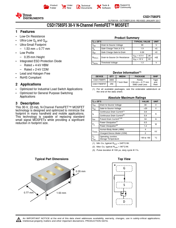
- Ultra-Small Footprint
- 1.53 mm × 0.77 mm
- Low Profile
- 0.35-mm Height
- Integrated ESD Protection Diode
- Rated > 4-k V HBM
- Rated > 2-k V CDM
- Lead and Halogen Free
- Ro HS pliant
2 Applications
- Optimized for Industrial Load Switch Applications
- Optimized for General Purpose Switching
Applications
3 Description
This 30-V, 22-mΩ, N-Channel Femto FET™ MOSFET technology is designed and optimized to minimize the footprint in many handheld and mobile applications. This technology is capable of replacing standard small signal MOSFETs while providing a significant reduction in footprint size.
.
.
.
.
.
.
Product Summary
TA = 25°C VDS Drain-to-Source Voltage Qg Gate Charge Total (4.5 V) Qgd Gate Charge Gate-to-Drain
RDS(on) Drain-to-Source On Resistance
VGS(th) Threshold Voltage
TYPICAL VALUE
VGS = 4.5 V VGS = 10 V
26 22
UNIT V n C n C mΩ
DEVICE CSD17585F5 CSD17585F5T
Device...