CSD23382F4
Description
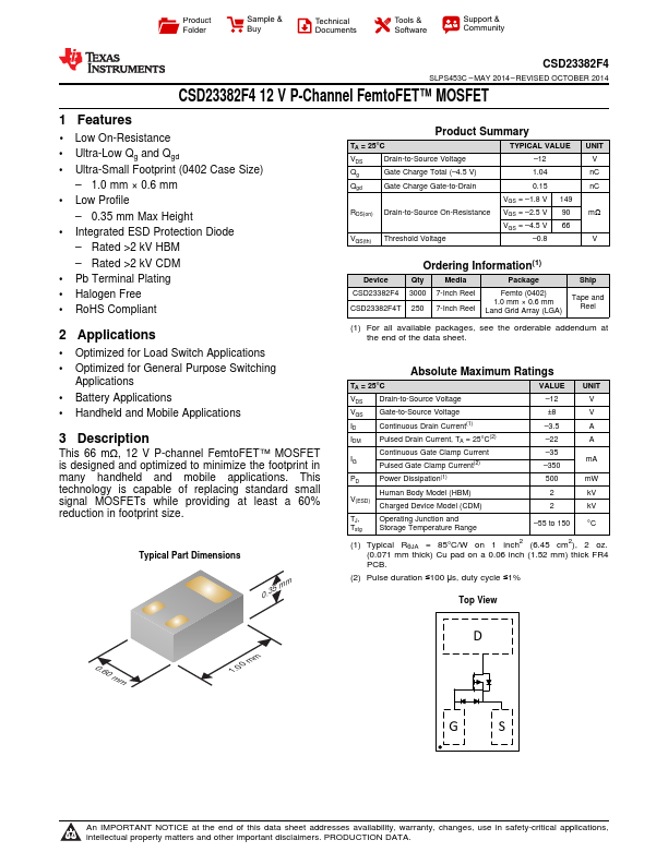
This 66 mΩ, 12 V P-channel FemtoFET™ MOSFET is designed and optimized to minimize the footprint in many handheld and mobile applications. This technology is capable of replacing standard small signal MOSFETs while providing at least a 60% reduction in footprint size. .
Key Features
- 1 Low On-Resistance
- Ultra-Low Qg and Qgd
- Ultra-Small Footprint (0402 Case Size) - 1.0 mm × 0.6 mm
- Low Profile - 0.35 mm Max Height
- Integrated ESD Protection Diode - Rated >2 kV HBM - Rated >2 kV CDM
- Pb Terminal Plating
- Halogen Free
- RoHS Compliant