CSD23382F4T
CSD23382F4T is P-Channel Power MOSFET manufactured by Texas Instruments.
- Part of the CSD23382F4 comparator family.
- Part of the CSD23382F4 comparator family.
Product Folder
Sample & Buy
Technical Documents
Tools & Software
Support & munity
CSD23382F4
SLPS453C
- MAY 2014
- REVISED OCTOBER 2014
CSD23382F4 12 V P-Channel FemtoFET™ MOSFET
1 Features
- 1 Low On-Resistance
- Ultra-Low Qg and Qgd
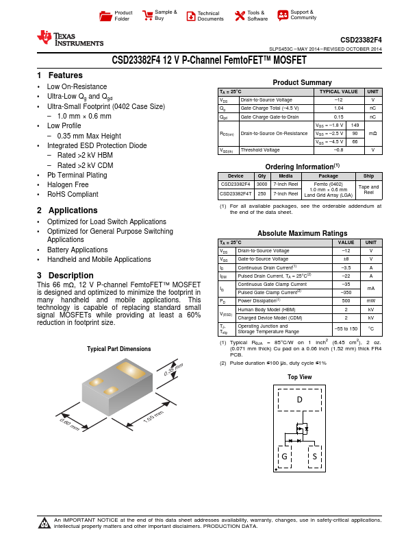
- Ultra-Small Footprint (0402 Case Size)
- 1.0 mm × 0.6 mm
- Low Profile
- 0.35 mm Max Height
- Integrated ESD Protection Diode
- Rated >2 kV HBM
- Rated >2 kV CDM
- Pb Terminal Plating
- Halogen Free
- RoHS pliant
2 Applications
- Optimized for Load Switch Applications
- Optimized for General Purpose Switching
Applications
- Battery Applications
- Handheld and Mobile Applications
3...