Datasheet Summary
.ti.
SLPS209A
- AUGUST 2009
- REVISED MAY 2010
P-Channel NexFET™ Power MOSFET
Check for Samples: CSD23201W10
Features
- Ultra Low Qg and Qgd
- Small Footprint 1mm × 1mm
- Low Profile 0.62mm Height
- Pb Free
- Gate ESD Protection
- 3kV
- RoHS pliant
- Halogen Free
APPLICATIONS
- Battery Management
- Load Switch
- Battery Protection
DESCRIPTION
The device has been designed to deliver the lowest on resistance and gate charge in the smallest outline possible with excellent thermal characteristics in an ultra low profile.
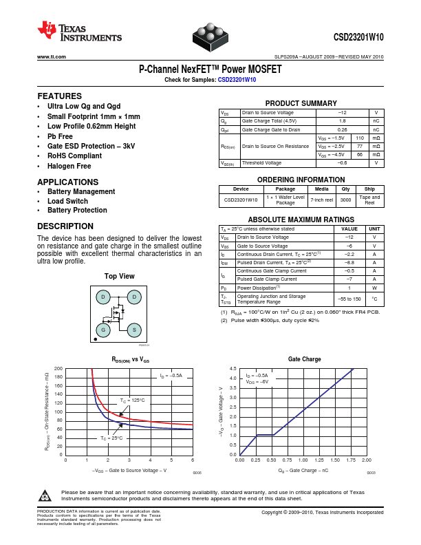
Top View
PRODUCT SUMMARY
Drain to Source Voltage
- 12
Qg
Gate Charge Total (4.5V)
1.8 nC
Qgd
Gate Charge Gate to...