CSD25303W1015 Overview
Key Specifications
Mount Type: Surface Mount
Pins: 6
Max Operating Temp: 150 °C
Min Operating Temp: -55 °C
Description
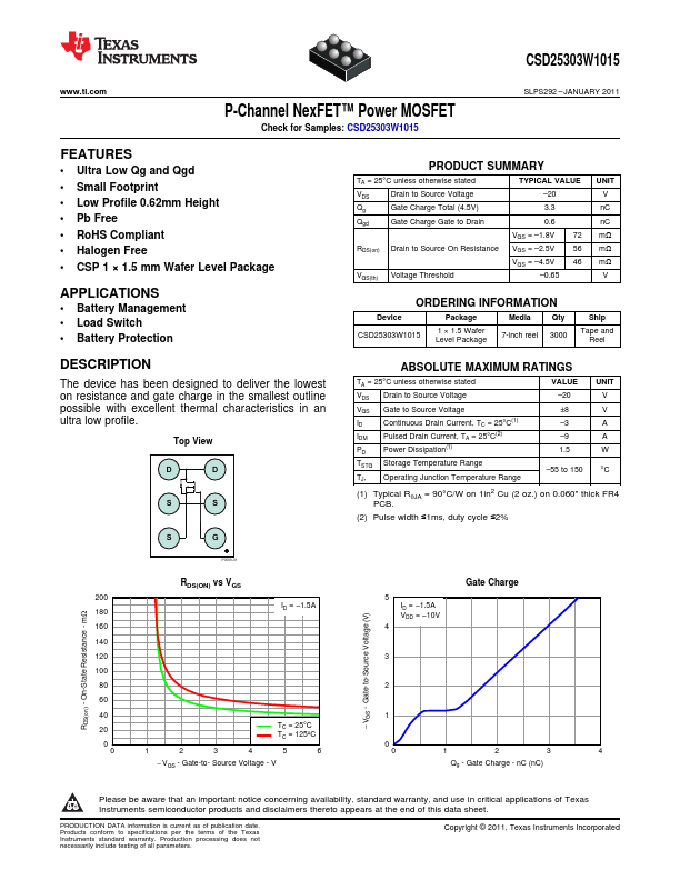
The device has been designed to deliver the lowest on resistance and gate charge in the smallest outline possible with excellent Top View D D S S S G PRODUCT SUMMARY TA = 25°C unless otherwise stated VDS Drain to Source Voltage Qg Gate Charge Total (4.5V) Qgd Gate Charge Gate to Drain RDS(on) Drain to Source On Resistance VGS(th) Voltage Threshold TYPICAL VALUE –20 3.3 0.6 VGS = –1.8V 72 VGS = –2.5V 56 VGS = –4.5V 46 –0.65 UNIT V nC nC mΩ mΩ mΩ V.
Key Features
- Ultra Low Qg and Qgd
- Small Footprint
- Low Profile 0.62mm Height
- RoHS Compliant
- Halogen Free