SN54BCT374FK Overview
Description
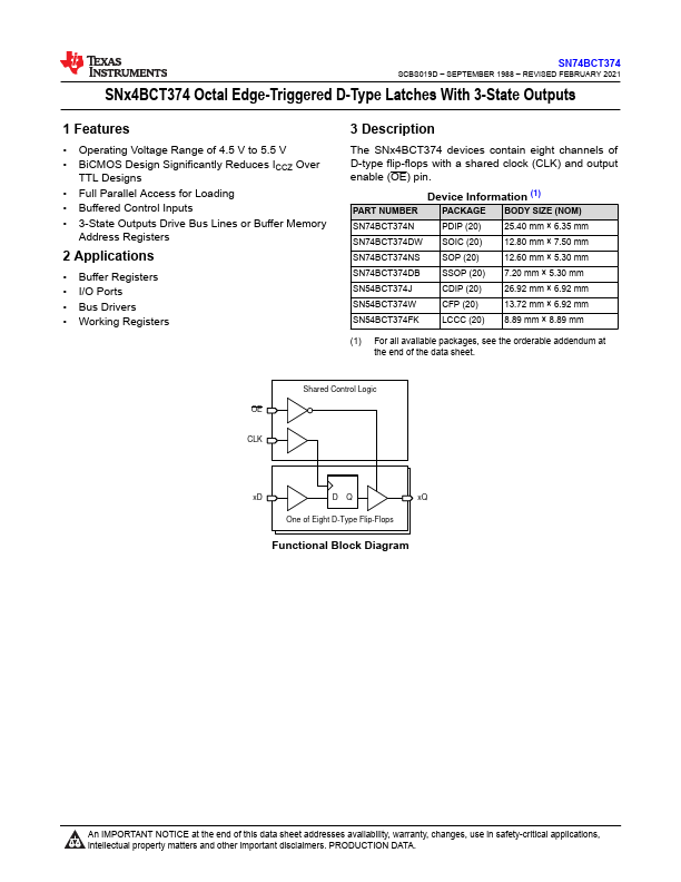
The SNx4BCT374 devices contain eight channels of D-type flip-flops with a shared clock (CLK) and output enable (OE) pin. Device Information (1) PART NUMBER PACKAGE BODY SIZE (NOM) SN74BCT374N PDIP (20) 25.40 mm × 6.35 mm SN74BCT374DW SOIC (20) 12.80 mm × 7.50 mm SN74BCT374NS SOP (20) 12.60 mm × 5.30 mm SN74BCT374DB SSOP (20) 7.20 mm × 5.30 mm SN54BCT374J CDIP (20) 26.92 mm × 6.92 mm SN54BCT374W CFP (20) 13.72 mm × 6.92 mm SN54BCT374FK LCCC (20) 8.89 mm × 8.89 mm (1) For all available packages, see the orderable addendum at the end of the data sheet.
Key Features
- Operating Voltage Range of 4.5 V to 5.5 V
- BiCMOS Design Significantly Reduces ICCZ Over TTL Designs
- Full Parallel Access for Loading
- Buffered Control Inputs
- 3-State Outputs Drive Bus Lines or Buffer Memory Address Registers