SN54LV126A Overview
Description
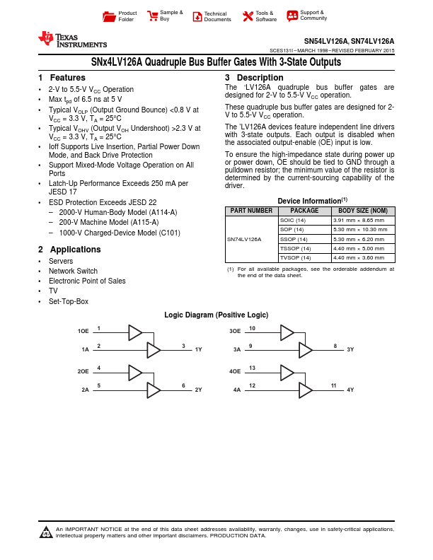
The ‘LV126A quadruple bus buffer gates are designed for 2-V to 5.5-V VCC operation. These quadruple bus buffer gates are designed for 2V to 5.5-V VCC operation.
Key Features
- 1 2-V to 5.5-V VCC Operation
- Max tpd of 6.5 ns at 5 V
- Typical VOLP (Output Ground Bounce) <0.8 V at VCC = 3.3 V, TA = 25°C
- Typical VOHV (Output VOH Undershoot) >2.3 V at VCC = 3.3 V, TA = 25°C
- Ioff Supports Live Insertion, Partial Power Down Mode, and Back Drive Protection
- Support Mixed-Mode Voltage Operation on All Ports
- Latch-Up Performance Exceeds 250 mA per JESD 17
- ESD Protection Exceeds JESD 22 – 2000-V Human-Body Model (A114-A) – 200-V Machine Model (A115-A) – 1000-V Charged-Device Model (C101)