SN74AUC2G06 Description
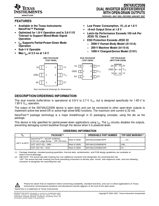
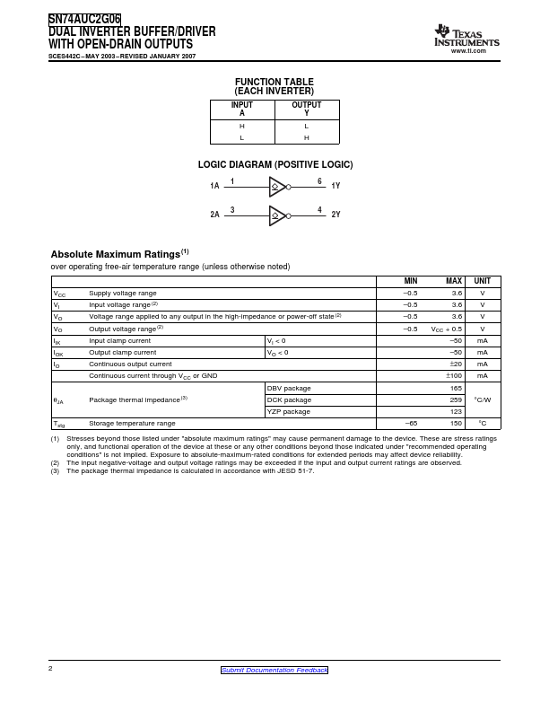
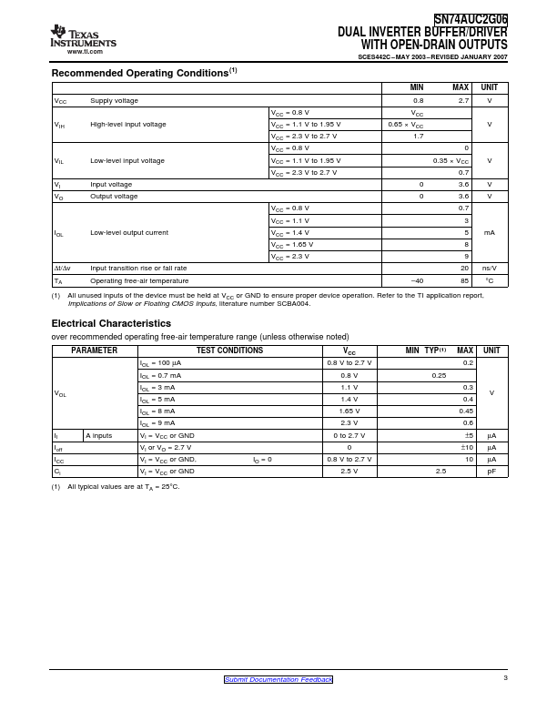
/ORDERING INFORMATION This dual inverter buffer/driver is operational at 0.8-V to 2.7-V VCC, but is designed specifically for 1.65-V to 1.95-V VCC operation. The output of the SN74AUC2G06 device is open drain and can be connected to other open-drain outputs to implement active-low wired-OR or active-high wired-AND functions. The maximum sink current is 32 mA.
SN74AUC2G06 Key Features
- Available in the Texas Instruments NanoFree™ Package
- Optimized for 1.8-V Operation and Is 3.6-V I/O Tolerant to Support Mixed-Mode Signal Operation
- Ioff Supports Partial-Power-Down Mode Operation
- Sub-1-V Operable
- Max tpd of 2.5 ns at 1.8 V
- MAY 2003
- REVISED JANUARY 2007
- Low Power Consumption, 10 µA at 1.8 V
- ±8-mA Output Drive at 1.8 V
- ESD Protection Exceeds JESD 22