SN74LVC1G125-Q1 Description
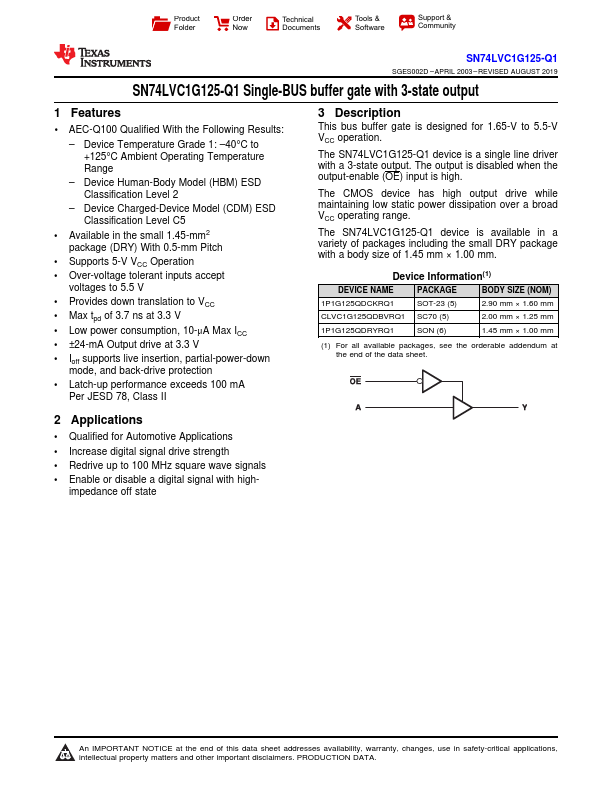
This bus buffer gate is designed for 1.65-V to 5.5-V VCC operation. The SN74LVC1G125-Q1 device is a single line driver with a 3-state output. The output is disabled when the output-enable (OE) input is high.
SN74LVC1G125-Q1 Key Features
- 1 AEC-Q100 Qualified With the Following Results
- Device Temperature Grade 1: -40°C to +125°C Ambient Operating Temperature Range
- Device Human-Body Model (HBM) ESD Classification Level 2
- Device Charged-Device Model (CDM) ESD Classification Level C5
- Available in the small 1.45-mm2 package (DRY) With 0.5-mm Pitch
- Supports 5-V VCC Operation
- Over-voltage tolerant inputs accept
- Provides down translation to VCC
- Max tpd of 3.7 ns at 3.3 V
- Low power consumption, 10-μA Max ICC
SN74LVC1G125-Q1 Applications
- Qualified for Automotive Applications