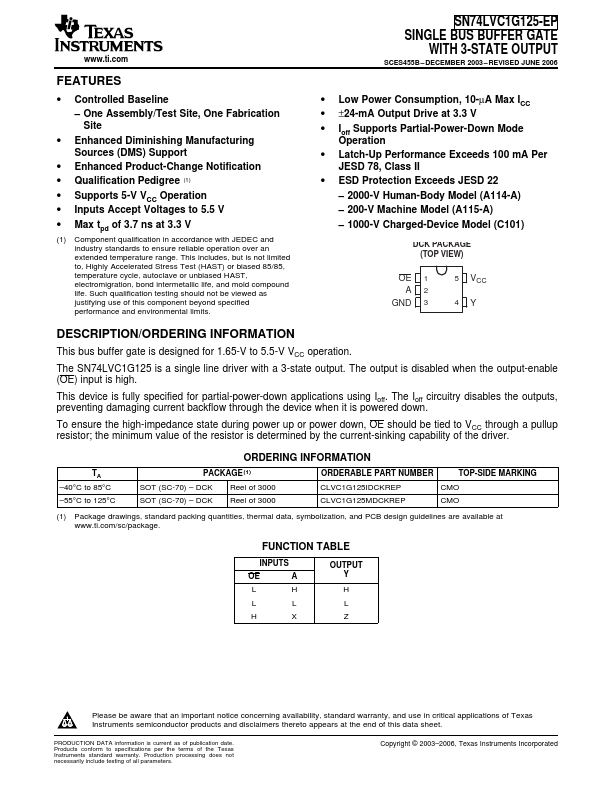
Datasheet4U Logo Datasheet4U.com

SN74LVC1G125-EP - Single Bus Buffer Gate

General Description

This bus buffer gate is designed for 1.65-V to 5.5-V VCC operation.

The SN74LVC1G125 is a single line driver with a 3-state output.

The output is disabled when the output-enable (OE) input is high.

Key Features

  • Controlled Baseline.
  • One Assembly/Test Site, One Fabrication Site.
  • Enhanced Diminishing Manufacturing Sources (DMS) Support.
  • Enhanced Product-Change Notification.
  • Qualification Pedigree (1).
  • Supports 5-V VCC Operation.
  • Inputs Accept Voltages to 5.5 V.
  • Max tpd of 3.7 ns at 3.3 V (1) Component qualification in accordance with JEDEC and industry standards to ensure reliable operation over an extended temperature range. This in.

📥 Download Datasheet

Full PDF Text Transcription (Reference)

The following content is an automatically extracted verbatim text from the original manufacturer datasheet and is provided for reference purposes only.

View original datasheet text
www.ti.com FEATURES • Controlled Baseline – One Assembly/Test Site, One Fabrication Site • Enhanced Diminishing Manufacturing Sources (DMS) Support • Enhanced Product-Change Notification • Qualification Pedigree (1) • Supports 5-V VCC Operation • Inputs Accept Voltages to 5.5 V • Max tpd of 3.7 ns at 3.3 V (1) Component qualification in accordance with JEDEC and industry standards to ensure reliable operation over an extended temperature range. This includes, but is not limited to, Highly Accelerated Stress Test (HAST) or biased 85/85, temperature cycle, autoclave or unbiased HAST, electromigration, bond intermetallic life, and mold compound life. Such qualification testing should not be viewed as justifying use of this component beyond specified performance and environmental limits.