SN74LVC1G125-Q1 Overview
Description
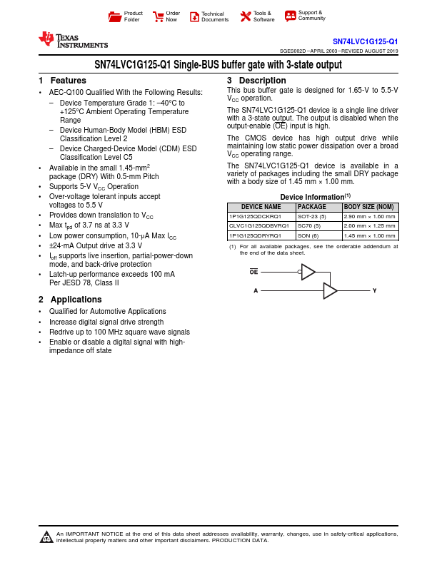
This bus buffer gate is designed for 1.65-V to 5.5-V VCC operation. The SN74LVC1G125-Q1 device is a single line driver with a 3-state output.
Key Features
- Available in the small 1.45-mm2 package (DRY) With 0.5-mm Pitch
- Supports 5-V VCC Operation
- Over-voltage tolerant inputs accept voltages to 5.5 V
- Provides down translation to VCC
- Max tpd of 3.7 ns at 3.3 V
- Low power consumption, 10-μA Max ICC
- ±24-mA Output drive at 3.3 V
- Ioff supports live insertion, partial-power-down mode, and back-drive protection
- Latch-up performance exceeds 100 mA Per JESD 78, Class II