SN74LVC2G06 Description
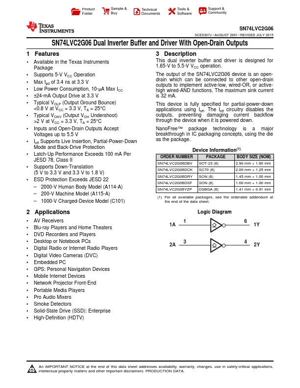
This dual inverter buffer and driver is designed for 1.65-V to 5.5-V VCC operation. The output of the SN74LVC2G06 device is an opendrain which can be connected to other open-drain outputs to implement active-low, wired-OR, or activehigh wired-AND functions. The maximum sink current is 32 mA.
SN74LVC2G06 Key Features
- 1 Available in the Texas Instruments Package
- Supports 5-V VCC Operation
- Max tpd of 3.4 ns at 3.3 V
- Low Power Consumption, 10-μA Max ICC
- ±24-mA Output Drive at 3.3 V
- Typical VOLP (Output Ground Bounce) <0.8 V at VCC = 3.3 V, TA = 25°C
- Typical VOHV (Output VOH Undershoot) >2 V at VCC = 3.3 V, TA = 25°C
- Inputs and Open-Drain Outputs Accept Voltages up to 5.5 V
- Ioff Supports Live Insertion, Partial-Power-Down Mode and Back-Drive Protection
- Latch-Up Performance Exceeds 100 mA Per JESD 78, Class II