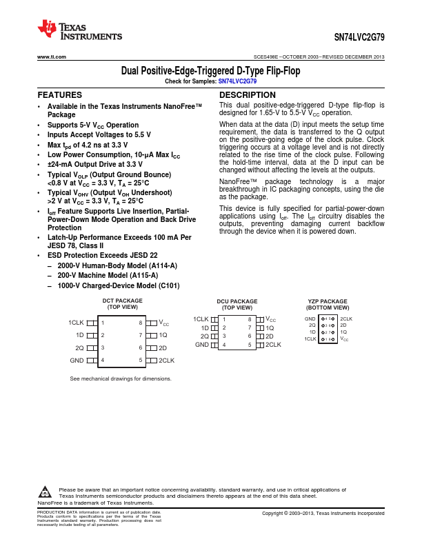
SN74LVC2G79 Description
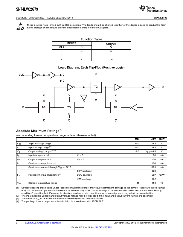
This dual positive-edge-triggered D-type flip-flop is designed for 1.65-V to 5.5-V VCC operation. When data at the data (D) input meets the setup time requirement, the data is transferred to the Q output on the positive-going edge of the clock pulse. Clock triggering occurs at a voltage level and is not directly related to the rise time of the clock pulse.
SN74LVC2G79 Key Features
- 2 Available in the Texas Instruments NanoFree™ Package
- Supports 5-V VCC Operation
- Inputs Accept Voltages to 5.5 V
- Max tpd of 4.2 ns at 3.3 V
- Low Power Consumption, 10-μA Max ICC
- ±24-mA Output Drive at 3.3 V
- Typical VOLP (Output Ground Bounce) <0.8 V at VCC = 3.3 V, TA = 25°C
- Typical VOHV (Output VOH Undershoot) >2 V at VCC = 3.3 V, TA = 25°C
- Ioff Feature Supports Live Insertion, PartialPower-Down Mode Operation and Back Drive Protection
- Latch-Up Performance Exceeds 100 mA Per JESD 78, Class II