TAS5755M
Overview
The TAS5755M is a single-chip flexible digital audio solution with integrated processing that supports 2.1 (2 speakers + subwoofer), 2.0 or stereo (2 speakers) and mono (high power speaker) modes. Its high efficiency, low 80 mΩ RDSON and pad-up package allows the device to output up to 2 × 50 W or 1 × 100 W.
- 1 Reduced Sol - Single-chip 2.1, 2.0 and Mono Mode Capable - Single-filter in Mono (PBTL) Mode. - Pad-up Package and 80 mΩ RDSON Enhances Thermal Performance
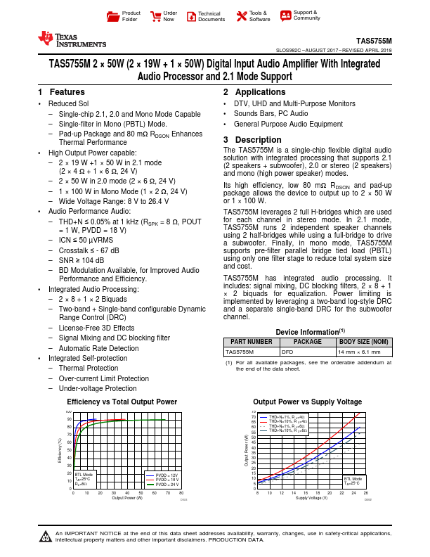
- High Output Power capable: - 2 × 19 W +1 × 50 W in 2.1 mode (2 × 4 Ω + 1 × 6 Ω, 24 V) - 2 × 50 W in 2.0 mode (2 × 6 Ω, 24 V) - 1 × 100 W in Mono Mode (1 × 2 Ω, 24 V) - Wide Voltage Range: 8 V to 26.4 V
- Audio Performance Audio: - THD+N ≤ 0.05% at 1 kHz (RSPK = 8 Ω, POUT = 1 W, PVDD = 18 V) - ICN ≤ 50 µVRMS - Crosstalk ≤ - 67 dB - SNR ≥ 104 dB - BD Modulation Available, for Improved Audio Performance and Efficiency.
- Integrated Audio Processing: - 2 × 8 + 1 × 2 Biquads - Two-band + Single-band configurable Dynamic Range Control (DRC) - License-Free 3D Effects - Signal Mixing and DC blocking filter - Automatic Rate Detection
- Integrated Self-protection - Thermal Protection - Over-current Limit Protection - Under-voltage Protection