• Part: TCM1030
  • Description: DUAL TRANSIENT-VOLTAGE SUPPRESSORS
  • Manufacturer: Texas Instruments
  • Size: 114.31 KB
Download TCM1030 Datasheet PDF
Texas Instruments
TCM1030
TCM1030 is DUAL TRANSIENT-VOLTAGE SUPPRESSORS manufactured by Texas Instruments.
description 
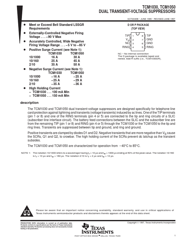
The TCM1030 and TCM1050 dual transient-voltage suppressors are designed specifically for telephone line card protection against lightning and transients (voltage transients) induced by ac lines. One of the TIP terminals (pin 1 or 8) and one of the RING terminals (pin 4 or 5) are connected to the tip and ring circuits of a SLIC (subscriber-line interface circuit). The battery feed connections between the SLIC and the subscriber line are from the remaining TIP (pin 1 or 8) and RING (pin 4 or 5) through the TCM1030 or the TCM1050 to the tip and ring lines. Transients are suppressed between tip and ground, and ring and ground. Positive transients are clamped by diodes D1 and D2. Negative transients that are more negative than VS cause the SCRs, Q1 and Q2, to crowbar. The high holding current of the SCRs prevent dc latchup as the transient subsides. The TCM1030 and TCM1050 are characterized for operation from - 40°C to 85°C. NOTE 1: The notation 10/1000 refers to a waveshape having tr = 10 µs and tw = 1000 µs ending at 50% of the peak value. The notation 10/160 is tr = 10 µs and tw = 160 µs. The notation 2/10 is tr = 2 µs and tw = 10 µs. Please be aware that an important notice concerning availability, standard warranty, and use in critical applications of Texas Instruments semiconductor products and disclaimers thereto appears at the end of this data sheet. PRODUCTION DATA information is current as of publication date. Products conform to specifications per the terms of Texas Instruments standard warranty. Production processing does not necessarily include testing of all parameters. - POST OFFICE BOX 655303 DALLAS, TEXAS 75265 Copyright © 1997, Texas Instruments Incorporated 1 TCM1030, TCM1050 DUAL TRANSIENT-VOLTAGE SUPPRESSORS SCTS040B - JUNE 1989 - REVISED JUNE 1997 functional block diagram 1 TIP 8 TIP 2 VS 4 RING Trip Circuit Trip Circuit D1 Q1 7 GND 6 GND Q2 D2 5 RING absolute maximum ratings over operating free-air temperature range (unless...