TLV733P-Q1
TLV733P-Q1 is LDO Linear Regulator manufactured by Texas Instruments.
Product Folder
Order Now
Technical Documents
Tools & Software
Support & munity
SBVS283E
- AUGUST 2016
- REVISED JULY 2019
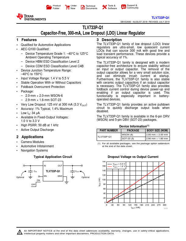
TLV733P-Q1 Capacitor-Free, 300-m A, Low Dropout (LDO) Linear Regulator
1 Features
- 1 Qualified for Automotive Applications
- AEC-Q100 Qualified:
- Device Temperature Grade 1:
- 40°C to 125°C Ambient Operating Temperature
- Device HBM ESD Classification Level 2
- Device CDM ESD Classification Level C4B
- Device Junction Temperature Range:
- 40°C to 150°C
- Input Voltage Range: 1.4 V to 5.5 V
- Stable Operation With or Without Capacitors
- Foldback Overcurrent Protection
- Package:
- 2.0-mm × 2.0-mm WSON-6
- 2.9-mm × 1.6-mm SOT-23
- Very Low Dropout: 125 m V at 300 m A (3.3 VOUT)
- Accuracy: 1% Typical, 1.4% Maximum
- Low IQ: 34 µA
- Available in Fixed-Output Voltages: 1.0 V to 3.3 V
- High PSRR: 50 d B at 1 k Hz
- Active Output...