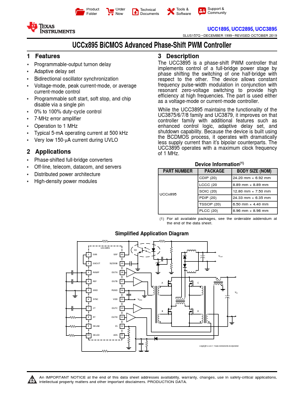
UCC1895, UCC2895, UCC3895
SLUS157Q – DECEMBER 1999 – REVISED OCTOBER 2019
www.ti.com
Table of Contents
1 Features .................................................................. 1
2 Applications ........................................................... 1
3 Description ............................................................. 1
4 Revision History..................................................... 2
5 Pin Configuration and Functions ......................... 3
6 Specifications......................................................... 5
6.1 Absolute Maximum Ratings ...................................... 5
6.2 ESD Ratings.............................................................. 5
6.3 Recommended Operating Conditions....................... 5
6.4 Thermal Information .................................................. 6
6.5 Electrical Characteristics........................................... 6
6.6 Typical Characteristics ............................................ 10
7 Detailed Description ............................................ 11
7.1 Overview ................................................................. 11
7.2 Functional Block Diagrams ..................................... 11
7.3 Feature Description................................................. 14
7.4 Device Functional Modes........................................ 17
7.5 Programming........................................................... 17
8 Application and Implementation ........................ 20
8.1 Application Information............................................ 20
8.2 Typical Application .................................................. 22
9 Power Supply Recommendations...................... 42
10 Layout................................................................... 42
10.1 Layout Guidelines ................................................. 42
10.2 Layout Example .................................................... 43
11 Device and Documentation Support ................. 44
11.1 Documentation Support ........................................ 44
11.2 Receiving Notification of Documentation Updates 44
11.3 Community Resource............................................ 44
11.4 Trademarks ........................................................... 44
11.5 Electrostatic Discharge Caution ............................ 45
11.6 Glossary ................................................................ 45
12 Mechanical, Packaging, and Orderable
Information ........................................................... 45
4 Revision History
NOTE: Page numbers for previous revisions may differ from page numbers in the current version.
Changes from Revision P (June 2013) to Revision Q
Page
• Added ESD Ratings table, Feature Description section, Device Functional Modes, Application and Implementation
section, Power Supply Recommendations section, Layout section, Device and Documentation Support section, and
Mechanical, Packaging, and Orderable Information section .................................................................................................. 1
• Changed UCC1895 VOL MAX, From 250 mV : To 300 mV in Electrical Characteristics ....................................................... 8
• Changed UCC1895 RAMP sink current MIN, From 12 mA : To 10 mA in Electrical Characteristics .................................... 8
• Changed the FSW note in the Detailed Design Procedure section ...................................................................................... 23
• Changed the voltage drop across the RDS(on) from 0.5-V to 4.5-V forward voltage drop in the output rectifiers.................. 23
• Added Output Voltage Setpoint section................................................................................................................................ 34
• Added Setting the Switching Frequency section .................................................................................................................. 36
• Added Soft Start section....................................................................................................................................................... 36
• Added Setting the Switching Delays section ........................................................................................................................ 36
• Added Setting the Slope Compensation section .................................................................................................................. 38
Changes from Revision O (April 2010) to Revision P
Page
• Added The CS input connects to text to the beginning of the CS Detailed Pin Description. ............................................... 14
• Added second paragraph to detailed REF Pin Description and included the UCC1895 at the end of the first
paragraph to differentiate capacitance capabilities of the devices. ...................................................................................... 16
• Changed UCC3895 Timing Diagram in the Application Information section to reflect the maximum duty cycle conditions 19
Changes from Revision N (May 2009) to Revision O
Page
• Changed REF pin description from “Do not use more than 1.0 μF of total capacitance on this pin.” to “Do not use
more than 4.7 μF of total capacitance on this pin.” .............................................................................................................. 16
2 Submit Documentation Feedback
Copyright © 1999–2019, Texas Instruments Incorporated
Product Folder Links: UCC1895 UCC2895 UCC3895