UCC28070-Q1
www.ti.com
SLUSA71A – JULY 2010 – REVISED JUNE 2011
INTERLEAVING CONTINUOUS CONDUCTION MODE PFC CONTROLLER
Check for Samples: UCC28070-Q1
FEATURES
1
• Qualified for Automotive Applications
• Interleaved Average Current-Mode PWM
Control with Inherent Current Matching
• Advanced Current Synthesizer Current
Sensing for Superior Efficiency
• Highly-Linear Multiplier Output with Internal
Quantized Voltage Feed-Forward Correction
for Near-Unity PF
• Programmable Frequency (30 kHz to 300 kHz)
• Programmable Maximum Duty-Cycle Clamp
• Programmable Frequency Dithering Rate and
Magnitude for Enhanced EMI Reduction
– Magnitude: 3 kHz to 30 kHz
– Rate: Up to 30 kHz
• External Clock Synchronization Capability
• Enhanced Load and Line Transient Response
through Voltage Amplifier Output Slew-Rate
Correction
• Programmable Peak Current Limiting
• Bias-Supply UVLO, Over-Voltage Protection,
Open-Loop Detection, and PFC-Enable
Monitoring
• External PFC-Disable Interface
• Open-Circuit Protection on VSENSE and
VINAC pins
• Programmable Soft Start
• 20-Lead TSSOP Package
DESCRIPTION
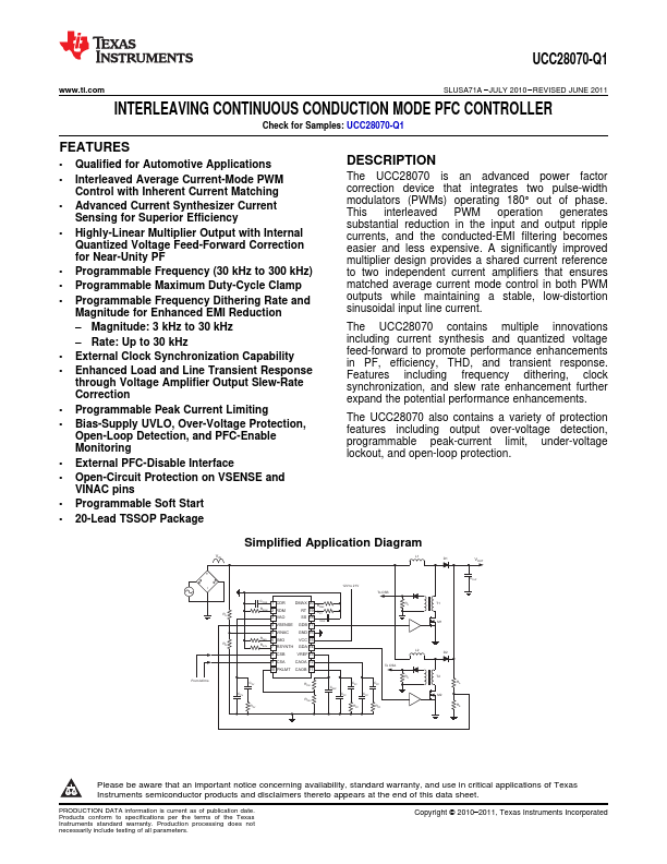
The UCC28070 is an advanced power factor
correction device that integrates two pulse-width
modulators (PWMs) operating 180° out of phase.
This interleaved PWM operation generates
substantial reduction in the input and output ripple
currents, and the conducted-EMI filtering becomes
easier and less expensive. A significantly improved
multiplier design provides a shared current reference
to two independent current amplifiers that ensures
matched average current mode control in both PWM
outputs while maintaining a stable, low-distortion
sinusoidal input line current.
The UCC28070 contains multiple innovations
including current synthesis and quantized voltage
feed-forward to promote performance enhancements
in PF, efficiency, THD, and transient response.
Features including frequency dithering, clock
synchronization, and slew rate enhancement further
expand the potential performance enhancements.
The UCC28070 also contains a variety of protection
features including output over-voltage detection,
programmable peak-current limit, under-voltage
lockout, and open-loop protection.
Simplified Application Diagram
V
IN
L1
D1
V
OUT
From Ixfrms
12V to 21V
To CSB
C
CDR
1 CDR
DMAX 20
R
DMX
R
RDM
2 RDM
RT 19
R
R RT
A
3 VAO
SS 18
C
SS
4 VSENSE GDB 17
R
S
5 VINAC GND 16
R
IMO
6 IMO
VCC 15
R
B
R
SYN
7 RSYNTH
GDA 14
8 CSB
VREF 13
L2
9 CSA CAOA 12
10 PKLMT CAOB 11
To CSA
C
ZV
C
PV
R
ZV
R
PK1
R
PK2
C
REF
C
PC
C
ZC
C
PC
C
ZC
R
ZC
R
ZC
R
S
C
OUT
T1
M1
D2
T2
R
A
M2
R
B
1
Please be aware that an important notice concerning availability, standard warranty, and use in critical applications of Texas
Instruments semiconductor products and disclaimers thereto appears at the end of this data sheet.
PRODUCTION DATA information is current as of publication date.
Products conform to specifications per the terms of the Texas
Instruments standard warranty. Production processing does not
necessarily include testing of all parameters.
Copyright © 2010–2011, Texas Instruments Incorporated