74AHCT2G241-Q100 Description
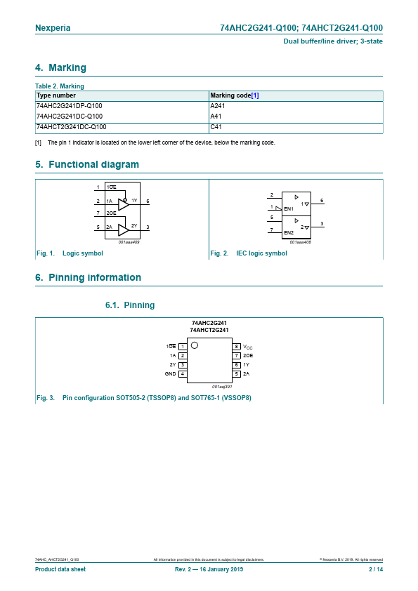
74AHCT2G241-Q100 is a high-speed Si-gate CMOS device. 74AHCT2G241-Q100 is a dual non-inverting buffer/line driver with 3state outputs. The 3-state outputs are controlled by the output enable inputs 1OE and 2OE.
74AHCT2G241-Q100 Key Features
- Automotive product qualification in accordance with AEC-Q100 (Grade 1)
- Specified from -40 °C to +85 °C and from -40 °C to +125 °C
- Symmetrical output impedance
- High noise immunity
- ESD protection
- MIL-STD-883, method 3015 exceeds 2000 V
- HBM JESD22-A114F exceeds 2000 V
- MM JESD22-A115-A exceeds 200 V (C = 200 pF, R = 0 Ω)
- Low power dissipation
- Balanced propagation delays
74AHCT2G241-Q100 Applications
- Automotive product qualification in accordance with AEC-Q100 (Grade 1)
- Specified from -40 °C to +85 °C and from -40 °C to +125 °C