74ALVC125-Q100 Description
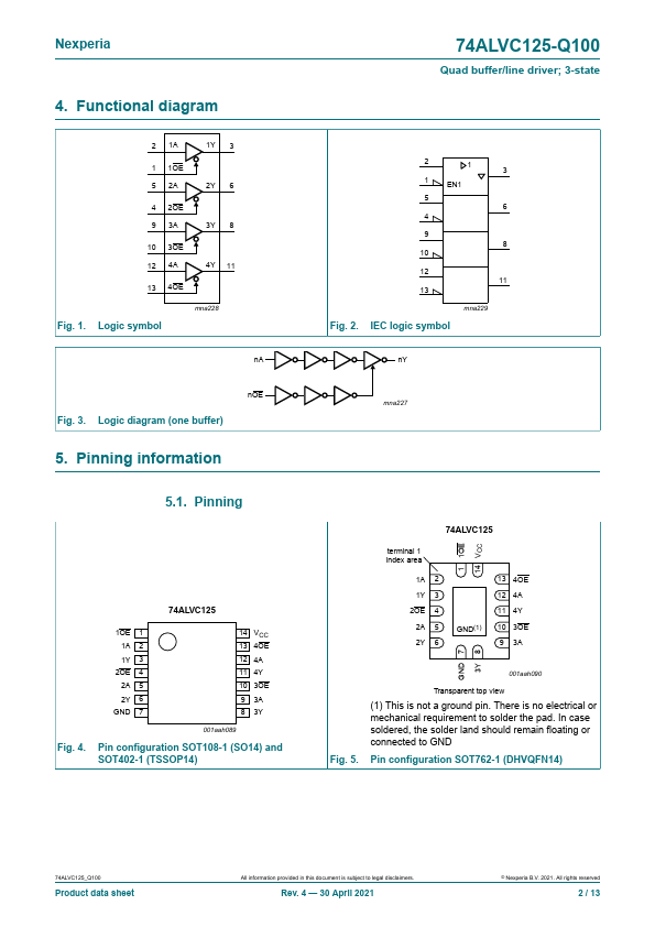
The 74ALVC125-Q100 is a quad non-inverting buffer/line driver with 3-state outputs. The 3-state outputs (nY) are controlled by the output enable input (nOE). A HIGH on the nOE pin causes the outputs to assume a high-impedance OFF-state.
74ALVC125-Q100 Key Features
- Automotive product qualification in accordance with AEC-Q100 (Grade 3)
- Specified from -40 °C to +85 °C
- Wide supply voltage range from 1.65 V to 3.6 V
- 3.6 V tolerant inputs/outputs
- CMOS low power consumption
- Direct interface with TTL levels (2.7 V to 3.6 V)
- Power-down mode
- Latch-up performance exceeds 250 mA
- plies with JEDEC standards
- JESD8-7 (1.65 V to 1.95 V)
74ALVC125-Q100 Applications
- Automotive product qualification in accordance with AEC-Q100 (Grade 3)
- Specified from -40 °C to +85 °C
- Wide supply voltage range from 1.65 V to 3.6 V